
"Turning waste into graphene" — what the Tohoku experiment actually fed the reactor
A genuine advance: graphene grown at around 300°C instead of 900°C. The waste-derived framing attached to it in coverage describes a step the experiment did not perform.
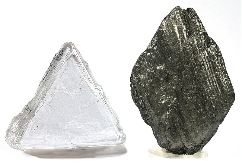
A Tohoku University result has been circulating under the heading of turning waste into graphene. The underlying paper is a good piece of work. The heading describes something else.
What the experiment did
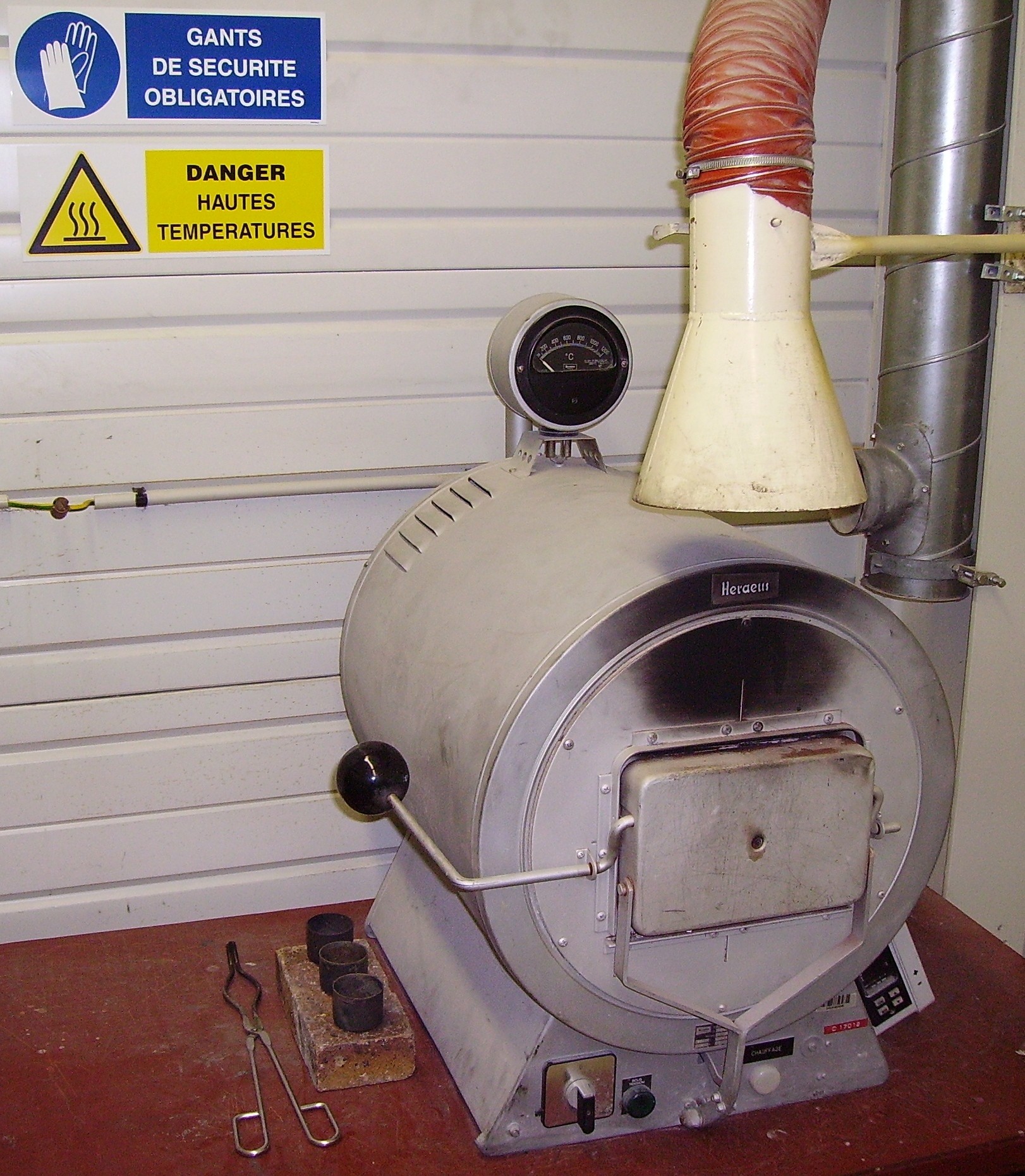
Chemical vapour deposition grows graphene by decomposing a carbon-containing gas over a catalytic surface. Conventionally that runs near 900°C — hot enough to constrain substrate choice, dominate the energy bill, and rule out direct growth on most electronics.
The Tohoku team demonstrated growth at approximately 300°C using acetylene as the carbon source.
That is a substantial result on its own terms. Lower temperature means cheaper furnaces, less energy per gram, and the possibility of depositing graphene directly onto temperature-sensitive substrates instead of growing it elsewhere and transferring it — transfer being the step that introduces most defects in practice.
What it did not do
The claim that would change the waste sector is "we made acetylene from waste and grew usable graphene from it." The published claim is "we grew graphene at 300°C from acetylene." Only one of those has been demonstrated.
The process turns waste into graphene.
The reactor was fed commercial acetylene. No waste material was converted to acetylene, and no waste-derived feedstock was tested in the study.
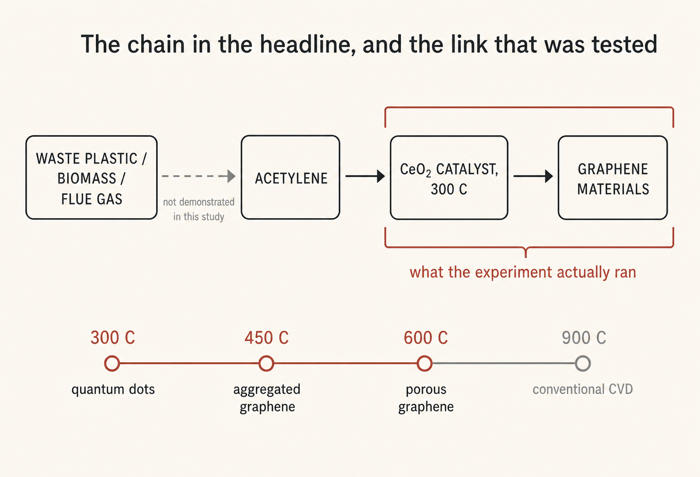
The waste connection is an inference: acetylene can in principle be produced from waste carbon — via calcium carbide, plasma pyrolysis of hydrocarbons, or gasification routes. All of those are energy-intensive, and none of them was demonstrated, costed, or characterised here.
That matters because the purity requirement is severe. CVD graphene quality is exquisitely sensitive to feedstock contaminants — sulphur, chlorine, and metals in particular. Waste-derived acetylene would need purification to semiconductor-adjacent specification before it entered the reactor, and the cost of that purification could easily exceed the cost of buying clean acetylene.
The other missing numbers
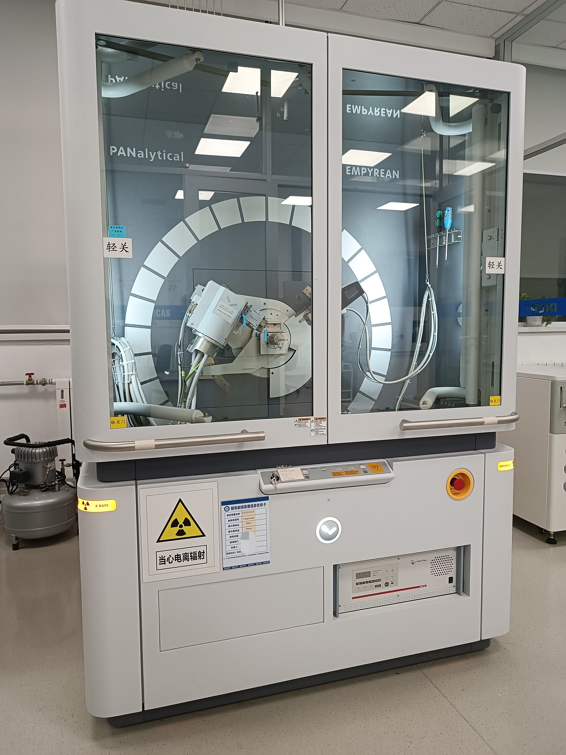
Lab-scale CVD tells you very little about manufacturability. Absent from the reporting: growth rate, film area, layer count and uniformity, defect density from Raman spectroscopy, carrier mobility, and yield.
There is also a market question that graphene coverage has been dodging for fifteen years. Graphene has been "about to transform" electronics, batteries, composites and membranes since 2010, and commercial volumes remain small relative to the promises. Even a much cheaper production route runs into the fact that demand at scale has not materialised in most of the announced applications.
And on the waste side: converting waste plastic to acetylene to graphene competes with mechanical recycling, pyrolysis to fuels, and simple energy recovery. Each of those has an existing cost structure. A route that ends in a low-volume speciality material needs the material's value to carry the whole chain.
The fair reading
A meaningful reduction in CVD growth temperature, worth attention on its own merits for flexible electronics and direct-on-device deposition.
It is not a waste-management result yet, and describing it as one skips the hardest step in the chain — the one where a mixed, dirty, variable feedstock has to become a gas pure enough to grow a crystal from.
References and image credits›
Photo: Robert M. Lavinsky, CC BY-SA 3.0 · Photo: via Wikimedia Commons, CC BY-SA · Photo: Jan Homann, CC BY-SA 4.0 · Photo: Grendelkhan, CC BY-SA 4.0, via Wikimedia Commons