
TNO's laser solar recycling: 99.998% silicon, unknown throughput
A nanosecond-laser process recovers silicon and silver from old panels at 97% rates and very high purity. The open questions are panels per hour and cracked real-world modules.
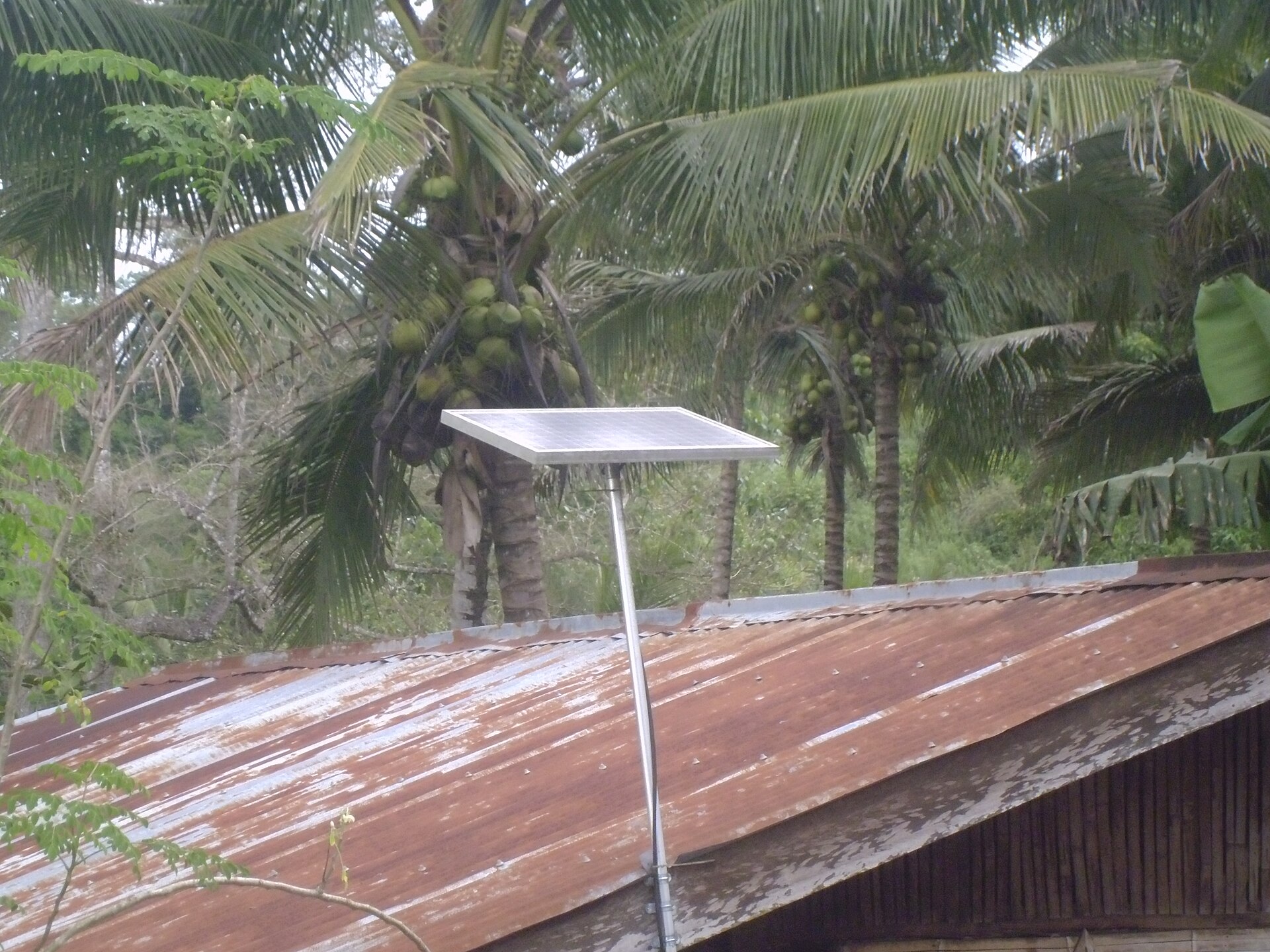
Most solar-panel recycling today recovers the easy parts — the aluminium frame and the glass — and loses or contaminates the valuable parts: the silicon and the silver. IRENA projects around 78 million tonnes of panel waste by 2050, so that gap is getting larger.
Researchers at TNO in the Netherlands, including Maarten van der Vleuten, presented a process called LARS (Laser Assisted Recycling of Solar Modules) at the SiliconPV conference. The headline numbers are striking. The question is whether they survive a factory.
How it works
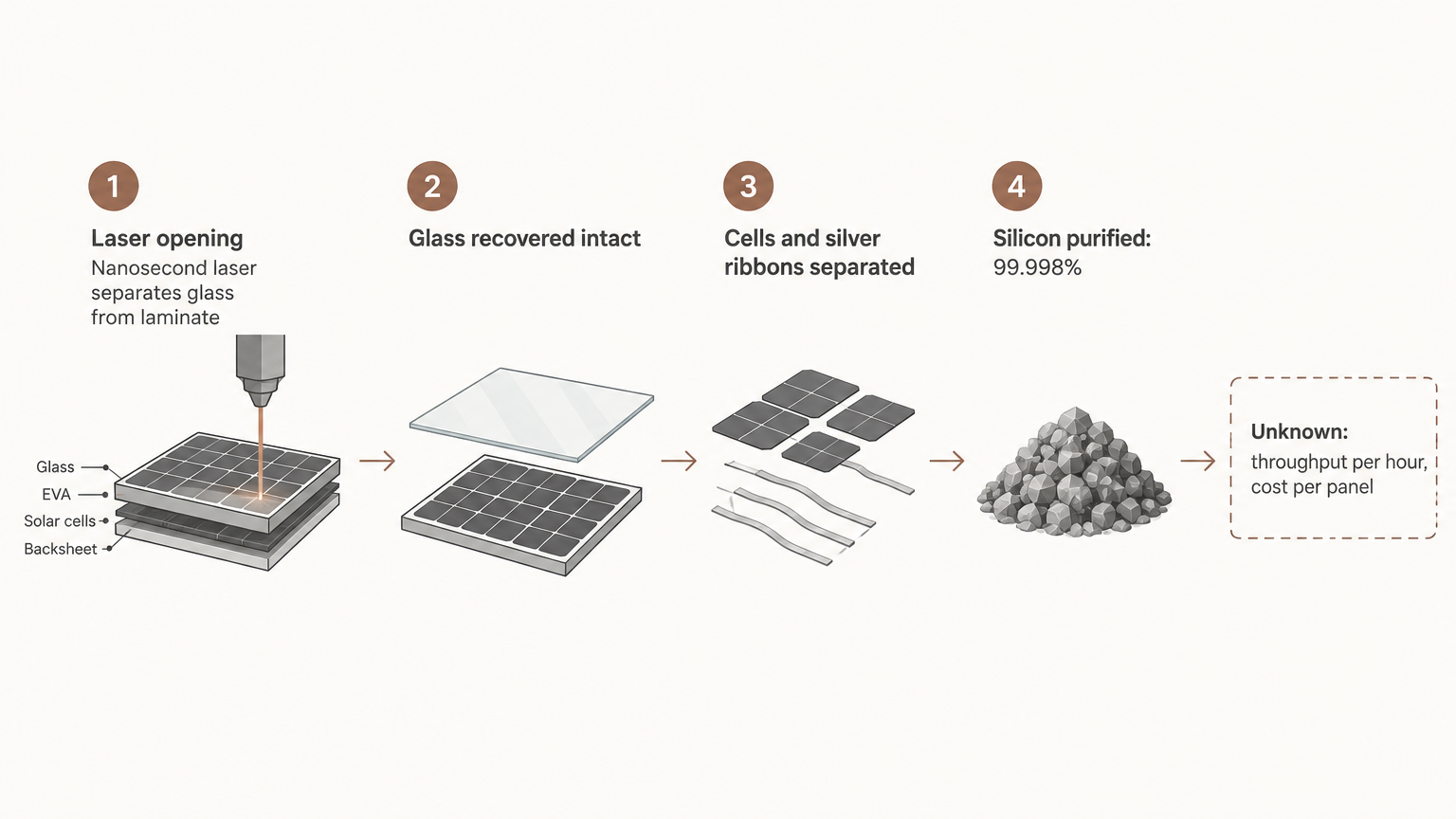
- Laser opening. A nanosecond laser separates the laminated layers without shattering the wafer. Shredding and chemical dissolution, by contrast, damage or contaminate the silicon.
- Coating removal. The same laser strips the silicon-nitride anti-reflective coating, which must go before the silicon can be reused.
- Wet chemical refining. Remaining contaminants are removed chemically.
- Silver recovery. The silver contacts are recovered too.
The reported results
- Silicon purity: up to 99.998%, at 97% recovery
- Silver purity: 99.7%, at 97% recovery
The promise
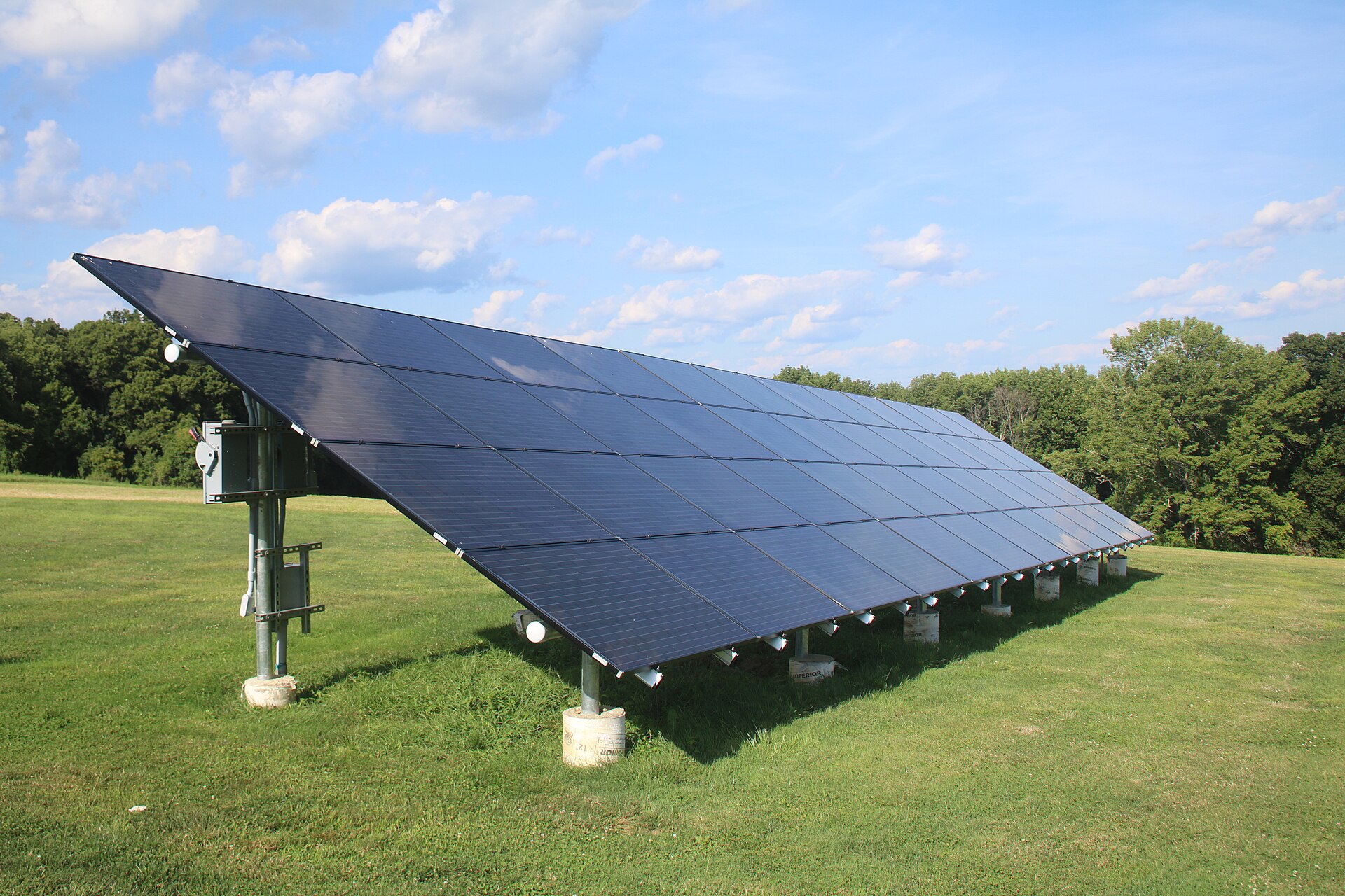
Silicon this pure could in principle return to new cell manufacturing. Silver is the most valuable material in a panel by weight, and 97% recovery at 99.7% purity is commercially attractive. Combining opening and coating removal in one laser step is a real simplification.
The catch
- Throughput. Results are from lab tests. A laser scanning a whole wafer surface may take minutes per panel. No panels-per-hour, cost or energy figure has been published, and recyclers handle millions of panels a year.
- Batch, not continuous. Each panel goes through opening, stripping and refining individually.
- Unnamed chemicals. The wet-refining chemicals and their waste stream are not specified.
- "Up to." 99.998% is the best result, not necessarily the typical one.
- Real panels are broken. Recovery depends on intact wafers. Many end-of-life panels are cracked by weather, transport or removal.
- Moving target. Newer cell designs (TOPCon, heterojunction) use different layers, and LARS was tuned for silicon-nitride coatings.
Laser recycling can recover high-purity silicon from end-of-life panels.
Purity is shown at lab scale. Throughput per hour and cost per panel, the numbers a recycler would pay for, are not yet public.
Sources
- PV Magazine — Laser-based PV recycling method demonstrates high silicon, silver recovery
- SiliconPV — LARS: Laser Assisted Recycling of Solar Modules
What matters more for panel recycling — purity or throughput?
References and image credits›
Photo: Bonvallite, CC BY-SA 3.0 · Diagram: The Waste Stack · Photo: Grendelkhan, CC BY-SA 4.0